Rabbit Zero Hold Time
Rabbit Semiconductor Technical Note 227 says, "However, the address hold time for the read cycle is quite small, nominally zero, but is usually positive because of capacitive loading on the address lines, which delays the address lines relative to the chip select and the read strobe." This "specification" makes it difficult to design a circuit that works correctly with variation of supply voltage and temperature.
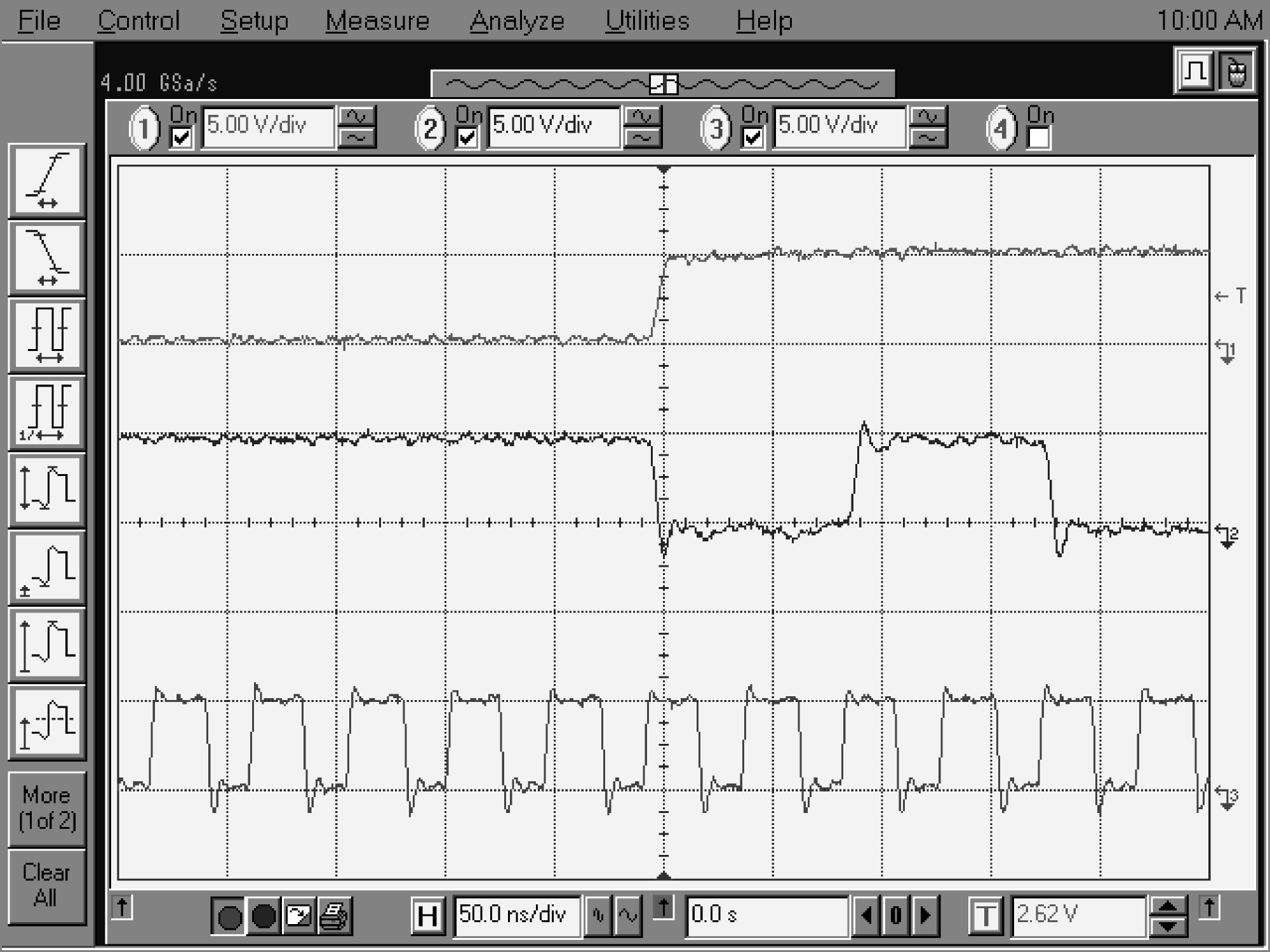
CH1: PE7 = CS*
CH2: A0
CH3: CLK
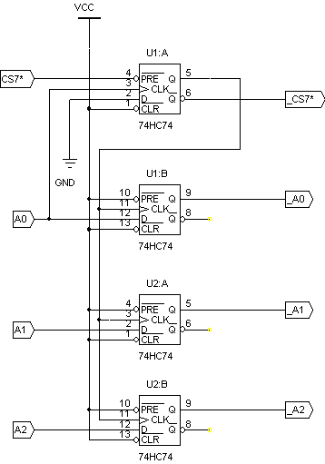
All we need to do is make sure that the address lines presented to the peripheral get latched before the end of the CS* assertion and that the latched CS* is negated soon after the IO cycle. This can be done by using A0 to clock a DFF.
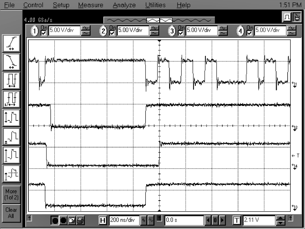
CH1: A0
CH2: IORD
CH3: PE7 = CS*
CH4: delayed CS*
Note that while not shown in the scope trace, _A0, the signal that drives the peripheral,
remains static at the level of A0 when CS* was asserted until the next assertion of CS*.